Ask Latest Price
Active Member
4 Years

Shenzhen Changkeshun Technology Co., Ltd.
Shenzhen Changkeshun Technology Co., Ltd.

Add to Cart
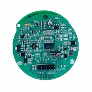
Best Sale Wireless Charger Pcba Circuit Board White Silk Bluetooth Multilayer PCBs
—————————————————————————————————————————————————————
CKS have fallen into this field for more 10years.With access to global suppliers, and distribution networks ,we source parts
for your assemblies as needed. Using our own in-house Stock and MRP system which links to our production data we
are able to manage Inventory levels, lead times and buffer stocks to meet your deadlines.
We are experienced in manufacturing a wide range of products including:
Telecommunication products
Safety devices
Home and office securities
Industrial and consumer electronics
Security Power Supply
Bluetooth speakers
LED lamp
Smart home products
Smart Bracelet & Watch
Electronic toys
Small Appliances
Specification of PCB Manufacturing
| Items | Paramerers |
| Double side/Mulyti-layer | |
| Max panel size | 32'*20'(800mm*508mm) |
| Minimum track/gap IL | 0.075mm/0.075mm(3mil/3mil) |
| Min annular ring on inner layer one side | 3mil(0.075mm) |
| Maximum Cu weight OL | 6oz(210um) |
| Maximum Cu weight 1L | 12oz(420um) |
| Finished board thickness | 0.20-6mm |
| Layer count | 2-32L |
| Layer to layer registration | ±3mil(±76um) |
| Min finished hole diameter | 0.15mm(6mil),0.1mm(4mil) for HDI |
| Hole position Accuracy | ±2mil(±50um) |
| Slot hloe Tolerance | ±3mil(±75um) |
| PTH diameter tolerance | ±2mil(±50um) |
| NPTH diameter tolerance | ±1mil(25±um) |
| Max Aspect ratio PTH | 10:1 |
| Copper on the wall of the holes | 0.4-2mil(10-50um) |
| Grapic pattern registration tolerance | ±3mil(0.075um) |
| Minimum track/gap 1L(mil)-copper weight dependant | 3mil/3mil(75um/75um) |
| The track Etching tolerance | ±1mil(±25um) |
Factory production lines:
